Shrike-fi: ESP32-S3 Meets FPGA on One Affordable Board
- ESP32-S3
- 1120 × 5-input LUT FPGA
- USB Type-C
- QSPI Flash 8 MB
- Optional QSPI PSRAM up to 8 MB
- Optional on-board BMS
- PMOD compatible connector
What You Will Build
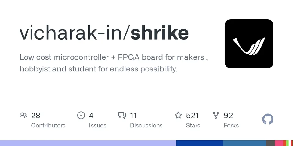
The Shrike-fi is the wireless member of Vicharak's Shrike family — a compact development board that combines an ESP32-S3 microcontroller with a 1120 × 5-input LUT FPGA on the same PCB. The two chips are wired together through a dedicated FPGA-to-MCU IO interface, so the ESP32-S3 can talk to custom digital logic you write in Verilog while simultaneously handling WiFi, BLE, and your application code.
This makes the board useful for projects that need both the flexibility of reconfigurable hardware (custom peripherals, signal processing pipelines, protocol bridges) and the convenience of a wireless-capable microcontroller. Because the hardware design and all toolchain software are fully open-source, you can inspect, modify, and contribute back every layer of the stack.
What You Need
Hardware
- Shrike-fi board (available from the Vicharak store; see the repository README for the direct link)
- USB Type-C cable (used for both power and programming)
- Optional: breadboard and jumper wires — the board is breadboard-compatible
- Optional add-ons (not pre-soldered on the base version): QSPI PSRAM up to 8 MB and an on-board BMS — these pads are present on the PCB and can be soldered yourself; see the hardware overview in the official documentation
Software
- The open-source toolchain provided by the Shrike project (see the documentation site for installation instructions)
- Your choice of language for the ESP32-S3: MicroPython, CircuitPython, or embedded C
- Verilog for FPGA logic
The full pinout, including the FPGA-to-ESP32-S3 communication pins, is published on the pinouts page.
Typical use cases
Work through one-concept-per-example Verilog tutorials with real hardware, then graduate to full projects without buying a second board.
Use the FPGA to handle custom sensor protocols or signal conditioning while the ESP32-S3 sends processed data over WiFi or BLE.
Implement timing-critical peripherals — PWM arrays, protocol bridges, state machines — in Verilog and free the ESP32-S3 for application logic.
Add the optional on-board BMS to build a self-contained wireless device that combines reconfigurable hardware with long-term deployment.
How It Works
The Shrike-fi architecture keeps the FPGA and the ESP32-S3 as peers on the same board rather than treating the microcontroller as a mere programmer.
- FPGA fabric — 1120 five-input LUTs give you enough logic to implement custom UART controllers, SPI slaves, PWM engines, state machines, or simple soft-processors in Verilog.
- ESP32-S3 host — handles WiFi, BLE, USB, and runs your application logic in MicroPython, CircuitPython, or C. It programs and configures the FPGA over the dedicated IO interface.
- FPGA ↔ MCU IO interface — a direct electrical connection between the two chips lets the ESP32-S3 pass data to and from whatever logic you load onto the FPGA, enabling tight cooperation between software and reconfigurable hardware.
- Shared resources — 8 MB of QSPI flash, two user LEDs, a PMOD-compatible connector for plug-in modules, and a USB Type-C port that handles both power delivery and programming for both chips.
- Optional PSRAM — up to 8 MB of QSPI PSRAM can be added to the base board by soldering the optional pads, expanding memory for data-hungry applications.
Build and Flash Steps
The README does not include inline terminal commands, so the steps below follow the documented workflow. Consult the official documentation for the exact commands matched to your OS.
- Get the board — order a Shrike-fi from the Vicharak store (link in the repository README).
- Set up the toolchain — follow the toolchain setup guide on the documentation site. Vicharak commits to keeping every piece of Shrike software open-source.
- Clone the repository and browse the examples — find the repository at github.com/vicharak-in/shrike. The
examples/folder is structured as one concept per example, making it a good starting point for learning the FPGA-MCU interaction. - Write or pick a Verilog design — open any example, read through the HDL, and modify it or start your own.
- Synthesise and upload the FPGA bitstream — use the project toolchain commands documented on the site to synthesise your Verilog and flash the FPGA over USB Type-C.
- Flash the ESP32-S3 — upload your MicroPython, CircuitPython, or C firmware to the ESP32-S3 using the same USB Type-C cable.
- Check pinouts — verify your connections against the pinouts page, paying attention to the FPGA-to-ESP32-S3 communication pins if your project uses the inter-chip interface.
- Test with the user LEDs — both LEDs are available as simple targets to confirm your bitstream loaded and your firmware is running before moving to more complex IO.
Example Projects and Community Builds
The Shrike repository separates teaching examples from full builds. The examples/ folder in the main repo covers individual concepts — a good place to learn. Finished projects live in the companion shrike_projects repository, where you can browse what others have made and submit your own.
Vicharak also runs occasional bounties for specific features or integrations; check bounty.md in the repository for active tasks.
The Vicharak community is active across Discord, Reddit, and their own discussion forum — all linked from the README — which is useful when you hit toolchain questions or want feedback on a design.
Ideas to Extend It and Limitations
Ideas to extend
- Add QSPI PSRAM (up to 8 MB) by soldering the optional pads on the base board — useful for buffering large sensor streams or audio data.
- Solder the optional on-board BMS to build a battery-powered wireless node that combines custom FPGA signal processing with ESP32-S3 WiFi reporting.
- Use the PMOD-compatible connector to attach standard PMOD modules (displays, ADCs, DACs, sensors) without custom wiring.
- Implement a custom SPI or UART peripheral in Verilog on the FPGA and drive it from MicroPython on the ESP32-S3, offloading timing-critical work from the microcontroller.
- Submit a project to the
shrike_projectsrepo and contribute examples back to the teaching collection.
Limitations to keep in mind
- The optional PSRAM and BMS are not pre-soldered on the base Shrike-fi; you need soldering skills and the correct components to enable them.
- The Shrike (RP2350 variant) and additional family members are still in development or crowdfunding, so documentation depth varies across variants.
- With 1120 LUTs the FPGA fabric is modest — sufficient for custom peripherals and learning, but not for large soft-CPU cores or complex DSP pipelines.
Shrike-fi is a genuinely useful board for anyone who wants to learn FPGA design without abandoning the familiar ESP32 ecosystem — the WiFi, BLE, and MicroPython support lower the entry barrier considerably. The fully open-source hardware and software stack, combined with a growing community and project repository, make it a solid long-term platform rather than a one-off dev kit. The modest 1120-LUT fabric keeps scope realistic for learning and peripheral offload, which is exactly what the board is designed for.
Sources
github.comvicharak-in/shrike — repository & README vicharak-in.github.ioOfficial websiteFacts in this article come from the project's public README and GitHub metadata at the time of writing. Images belong to their respective owners and link back to the original source.